- Solutions
Vision & Awareness
Detection & Tracking
Weapon System Vision
Optical modules for semiconductor & industrial
- Technologies
Design
Fibre Imaging
Image Processing
Wavelengths
- Products
- About
SOLUTIONS
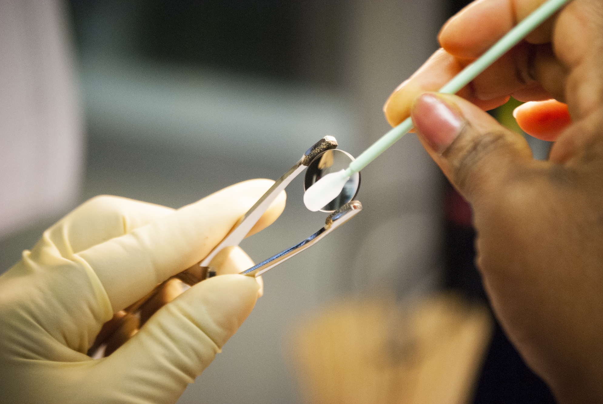
In the semiconductor market, Nedinsco specialises in complex optical systems, assemblies, measurement and control equipment, and alignment systems.
Nedinsco designs, develops and produces optical modules for alignment, measurement and control. Through its in-depth, in-house expertise, with a constant focus on the client, Nedinsco has impressive strengths in the semiconductor world. Nedinsco distinguishes itself with the supply of high-tech equipment that meets the demands of the semiconductor industry, both today and in the future.
A good example of this is the illuminator; an automated opto-mechatronic module with multiple optical elemenents that delivers delivers the homogenized light source in an advanced packaging lithography system. This critical module ensures high-resolution patterning, enabling the creation of intricate microstructures essential for modern semiconductor devices.
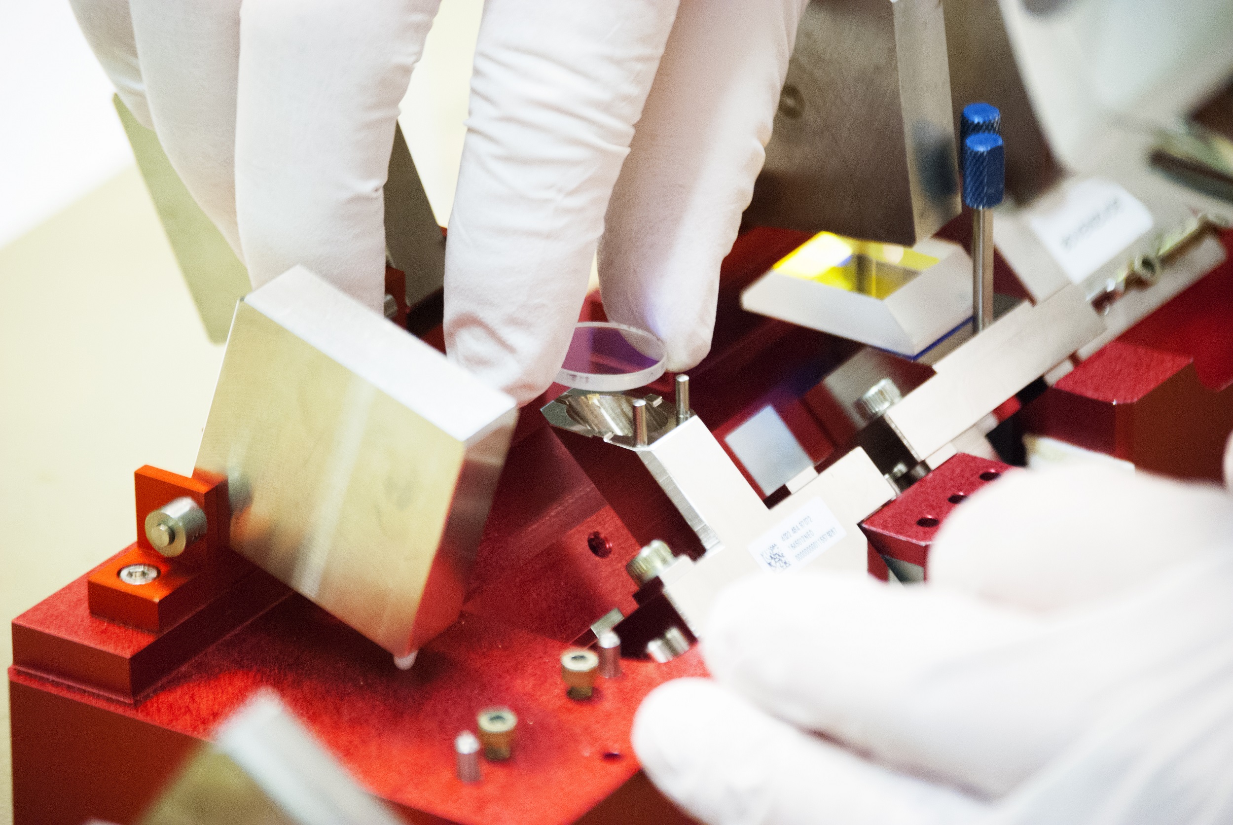

Nedinsco manufactures a variety of modules for semiconductor chip production, from individual components to fully integrated modules and tested systems with service and maintenance support. At Nedinsco, we provide a comprehensive range of services, carefully tailored to meet the specific needs of each client. With our advanced production capabilities, we ensure precision and are able to meet the industries’ challenging cleanliness requirements. Additionally, we are fully equipped to perform all measurements, testing and servicing in-house.
To meet increasingly challenging requirements in size, speed and cleanliness, Nedinsco proactively offers innovative solutions early in the development phase in close cooperation with our customer- and supplier base in Semicon.


By combining technical expertise, innovation, and collaboration, we provide advanced solutions designed to address the unique challenges of various industries effectively.
At Nedinsco, our Semiconductor solutions are built on proven technologies and customized to meet your specific requirements, ensuring you achieve excellence. Curious about how we turn your challenges into optimal solutions? Explore our approach to find out more.